Project Imu Array
Project IMU Array
System Arch
Quick Summary
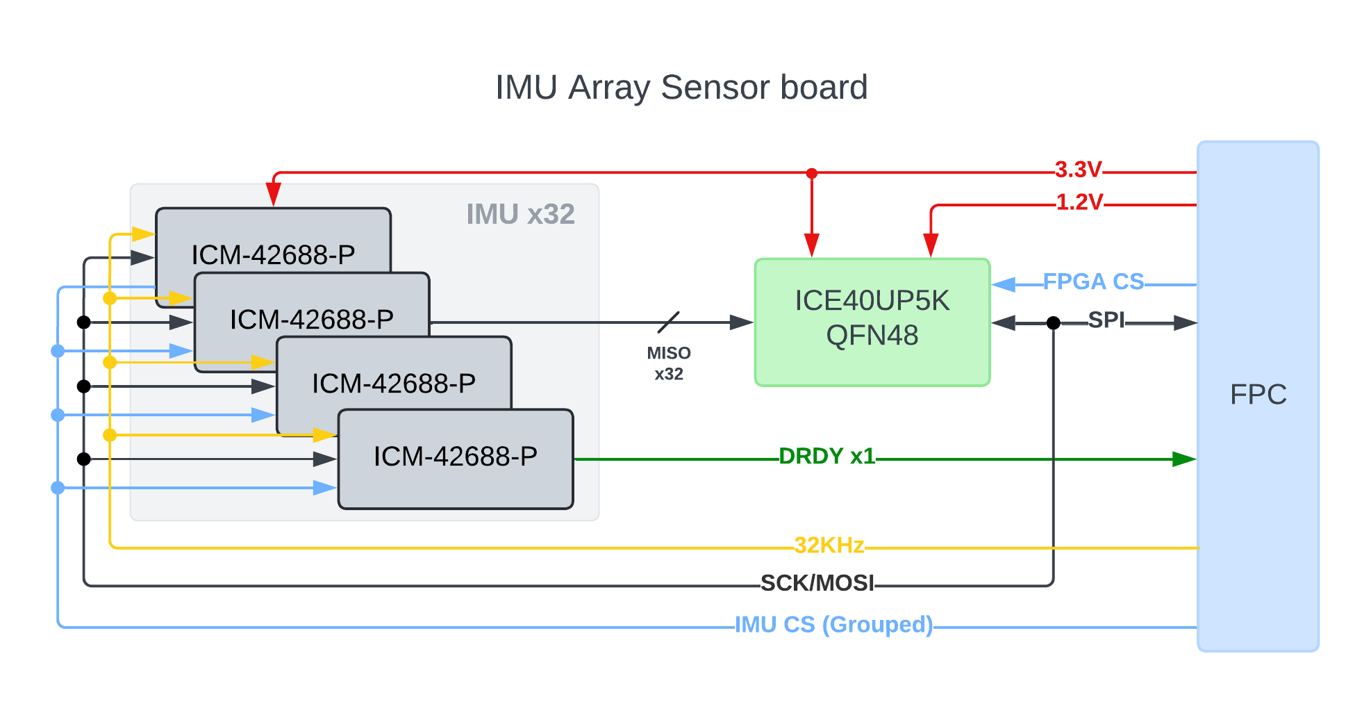
Before delving into the specifics, I would like to clarify a few points. Yes, I am utilizing an FPGA in this project, but its functionality is relatively straightforward and primarily serves as a data aggregator. The key to achieving synchronization among all the IMUs lies in the CLKIN function available in TDK/InvenSense’s IMU series. By synchronizing all the IMUs with a 32KHz clock using CLKIN, I can clock the internal synchronous logic of each IMU, ensuring that they all sample simultaneously. This synchronization simplifies the complexity of data processing by synchronizing all the samples after they have been collected.
Background
After I saw the board build by Sony, and realized that I’m probably not going to get the board because of the export control, I know that I’m going to build one myself because who doesn’t like an array of nicely packed PCB boards?
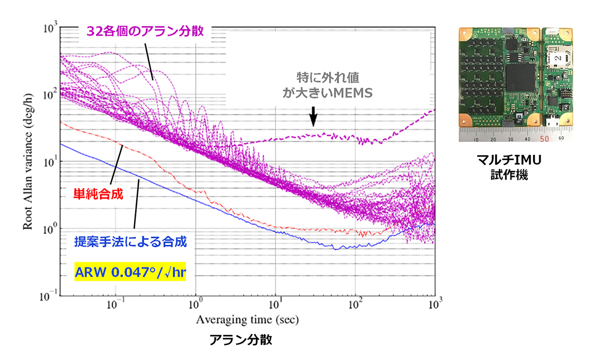 https://www.kenkai.jaxa.jp/research/innovation/multi_imu.html
The goal for me is to come up with geophone replacements. Ever since I deployed my seismometer project based on geophone, it always keeps me thinking on how to miniaturize the design and complexity. “Isn’t reading geophone as easy as tapping it with an ADC?” you might ask. The answer is yes (I’ve totally done that before), but the frequency response goes down in the lower ranges. The solution to extend frequency response is by NIC (Negative impedance converter), or put it simply, a negative resistance resistor, to cancel out geophones’ internal coil resistance. Which the seismometer project grows to involve multiple OPAs, digital potentiometers, and analog switches to implement NIC and its calibration circuits. (You can’t overcompensate, or it will oscillate.) It is so convoluted and trumptizing that to this day, I never bother to write it down.
Here is the main board for my seismometer project.
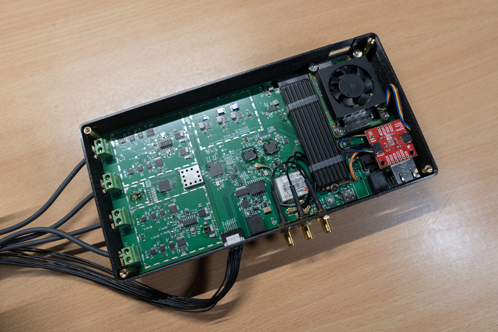 And this is the geophone sensor + Accelerometer.
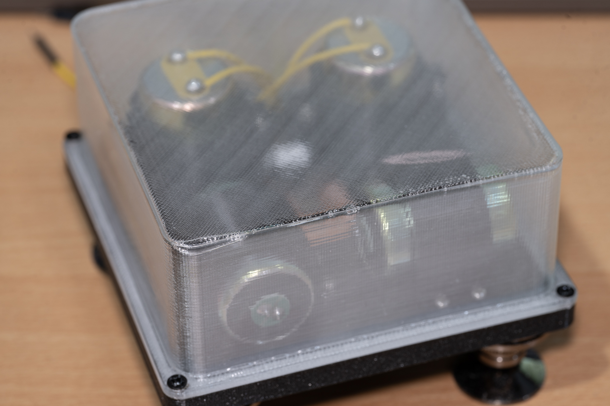
By using multiple IMUs and averaging out the noise, I’m hoping to finally get rid of all the analog components and expensive Analog Devices chipsets. This is also the reason why I’m probably not going to dive into the Gyro data or dynamic performance that much because that is not my main goal.
IMU Array
Hardware
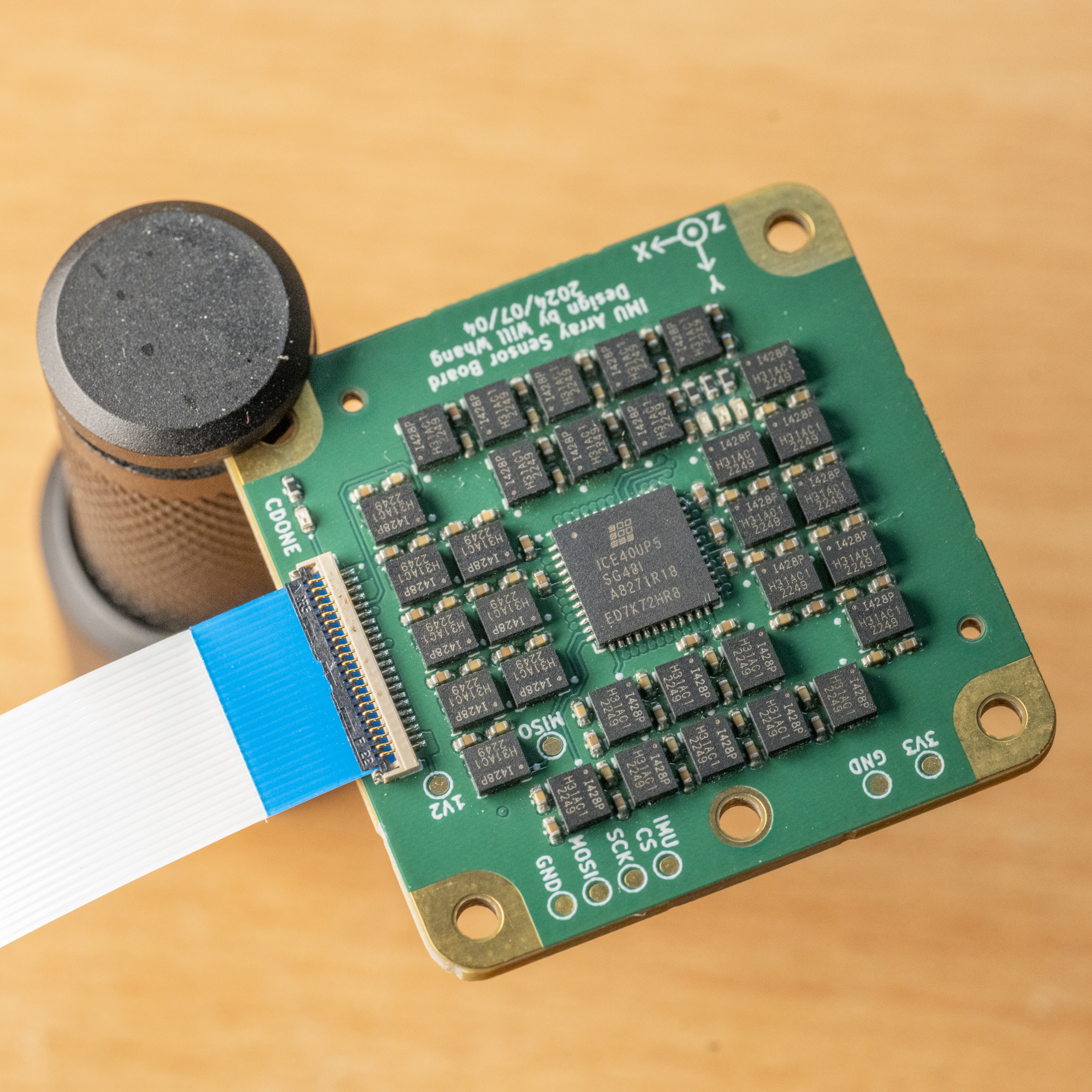
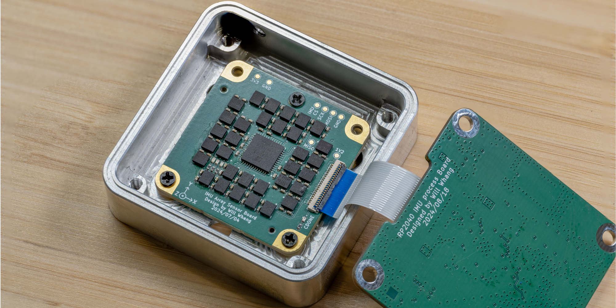
The goal is to make it as small as possible while still being flexible enough that it doesn’t require rework or costly respin of the board. I’m sending it directly to the PCBA without a prototype and adding complexiety will increase the risk. Also, since this sensor board is going to be expensive, I want to make sure I can reuse it as much as possible. So, I’m going to separate the processing board and the sensor board. The sensor board will be centered around an FPGA to make sure that even if I mess up the layout, I have the best chance of fixing it in the gateware.
Now the tricky part is how you place the IMUs - reading TDK’s layout guideline, my conclusion is that there is no fucking way to do it in the way that is not violating any of the rules, and I don’t know if anyone can put even a single IMU down on anything actual multiple components PCB board without any violation either, and this is just one single IMU. Moreover, for the array-related placements requirements specifically, if you look closer at Sony’s IMU array design, you can see that they group into a number of fours and rotate within the group; this is not for layout reasons but for canceling out the sensitivity differences for the axes.[reference pending]
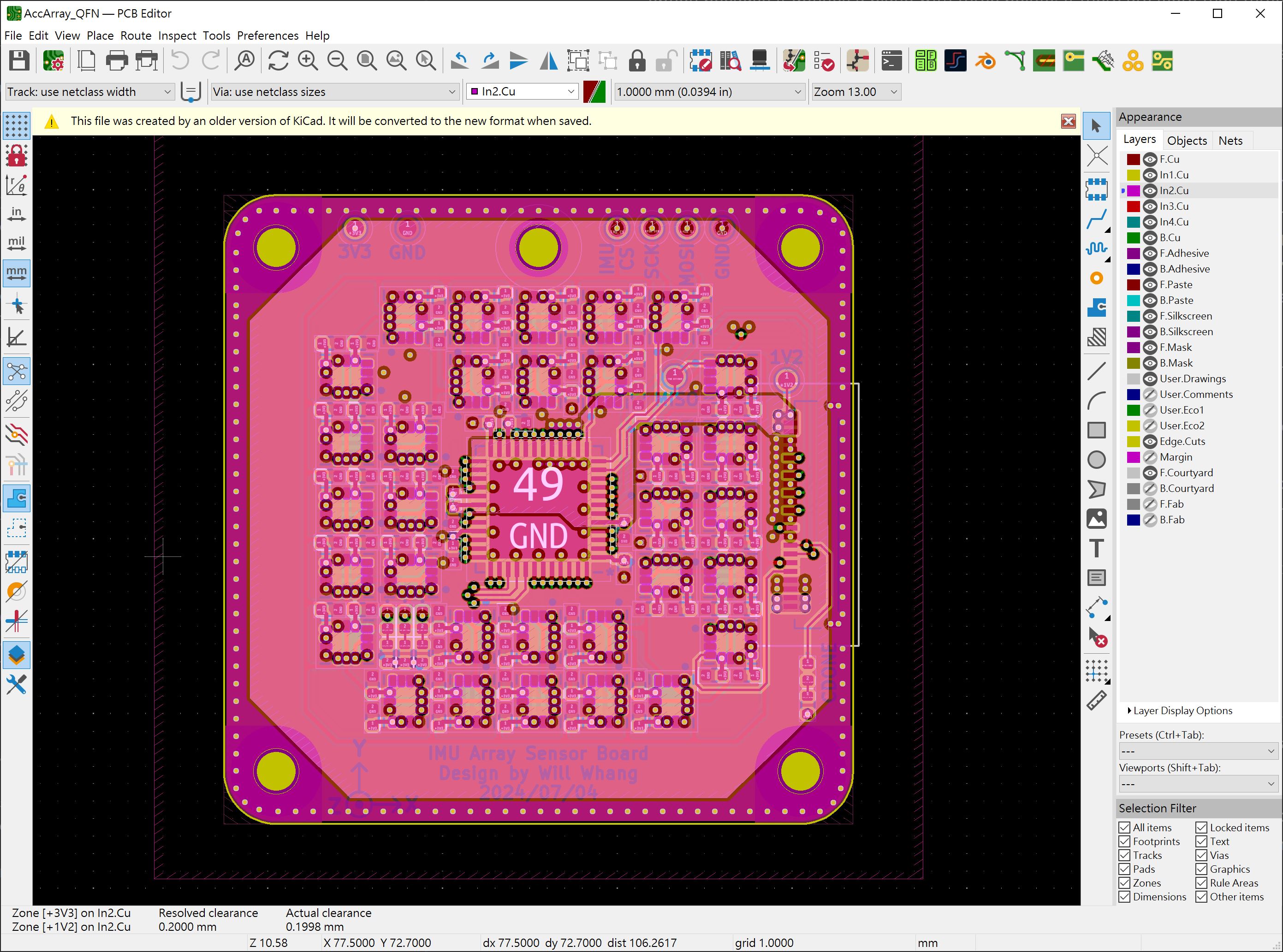
So, let’s put the compliant aside for now. According to the TDK layout guideline, I need to minimize mechanical stress as much as possible. A triangular mounting is the preferred option because it defines a plane with three points. If there are more than three mounting points, it introduces multiple planes, leading to increased mechanical stress on the PCB board. However, a triangle doesn’t work well with the four rotational placements required for the array. So, I’m still going with a square design, but I’ll reduce stress by not placing any IMUs on the diagonal line. But hey, after the placements and routing are done, I think I can squeeze in an extra screw hole for triangular mounting the board.
I’ve chosen the shallowest FPC connector I could find on Mouser because it’s the main factor limiting the board size (I want a square board). I also have a bunch of 22-pin FPC cables lying around for the RPI camera modules, so that’s the pin count I’ll use. Regarding the pinout, I’ve made sure to separate the SPI pins with ground pins for signal return. I don’t want to add any extra heat sources to the sensor board, so I’ve placed both 1.2V for the FPGA and 3.3V for the IMU/FPGA IO rails to the connector pins.
FPGA choice is a bit more difficult, mainly because the one I’m much familiar with (ICE40 series) doesn’t have any high pin count options for single row QFN. Originally, I had to opt with BGA ICE40HX as the result, but I realized that I’m able to get away with a lower cost ICE40UP5K 36 GPIO pin count. The SPI configuration port will double as SPI communication with the FPGA (so the FPGA bitstream needs to be uploaded from the host), so 32 for the IMU MISO and 4 for the SPI bus. The reason why datasheet stated it has 39 GPIOs is that the remaining 3 are designed for LEDs, which are output open drain only. Given that there is still some space left in the prohibited diagonal part of the board, I just put three LEDs as state machine indicators.
The downside is that FPGA cannot initiate the reading, as it doesn’t control the IMU CS pin, and doesn’t have any pin left for reading the IMU data ready pin either.
For the layout, this board is one of the few that I’ve decided to use more then 4 layers, it is needed for the compact sizes while maintaining good signal return path because it will be running at somewhat high (tens of Mhz) speed.
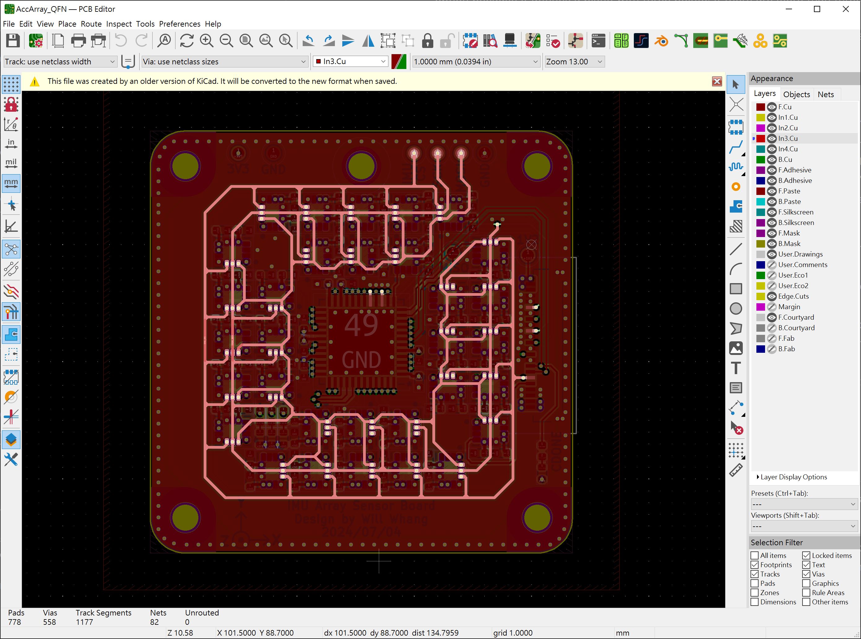
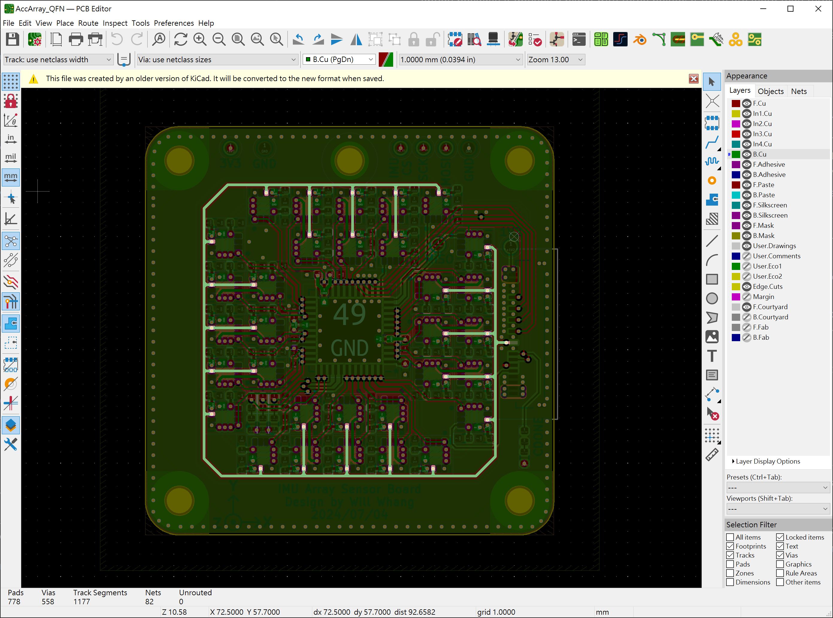
I utilized JLCPCB’s services for this board initially, but PCBWay subsequently approached me with a sponsorship offer and thus I am able to verify the board’s design with PCBWay’s services and have included the board files here if you want to order it.
Gateware
Now, let’s talk about how the reading is being done. The idea is as follows:
The MCU processes the IMU data as usual. Then, the FPGA reads the data from the internal buffer and stores it. Finally, the MCU retrieves the actual data from the buffer.
The FPGA will receive the first command/address byte and then decide whether to send the data out or read it from the IMUs.
This is what the logic trace looks like:

Originally the SPI logic is being driven by the 48MHz internal clock, but that limits the SPI transfer speed to be ~5MHz, so I’ve moved it to use the SPI clock directly (Async SPI core), which drastically increases the transfer speed to 20MHz, hooray!
But there is one critical catch: SPI bus is expecting the same data input and output phases, but because you can’t do both posedge and negedge at the same reg, there must be a cross clock domain process to send the data from posedge to negedge clock domain….. Or you just flip the settings in MCU and change the CPHA instead when reading. This is not an ideal solution, but it works for me, and I’ll just add that to the TODO list.
IMU Processing board
Hardware
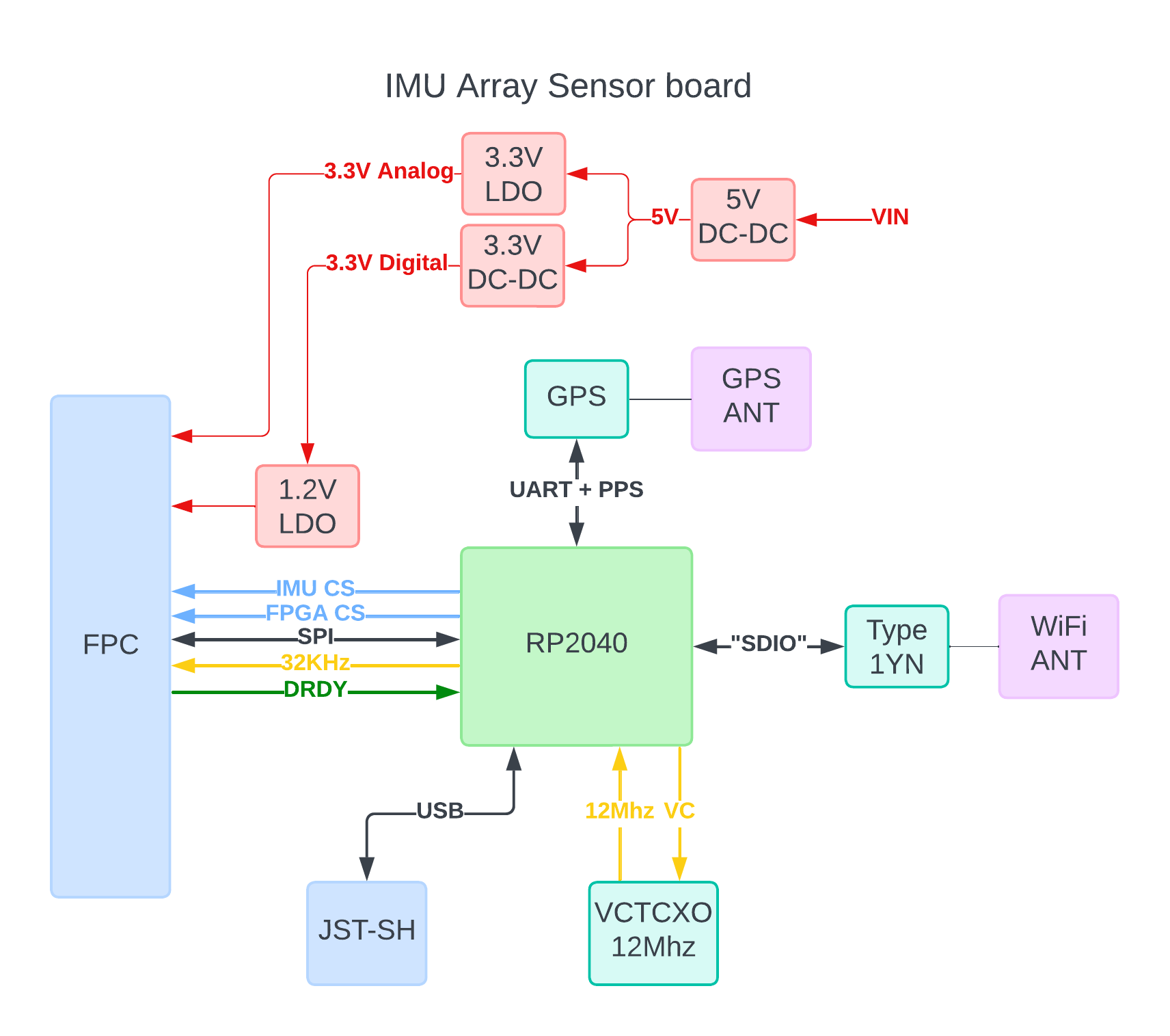
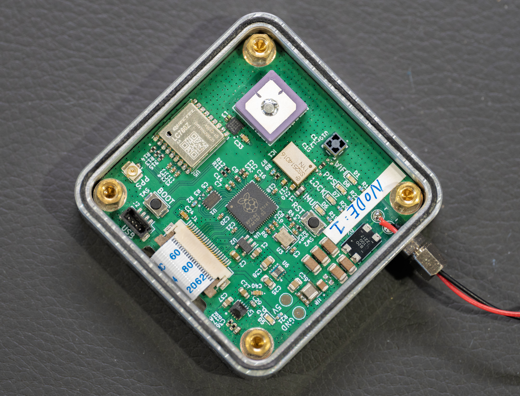
This will be the main data processing board, and my original plan is to use WiFi to transmit the data back since that in theory I just need < 1Mbps (200Hz x 512 bytes/measurements * 8 = 800 kpbs). Additionally, I will need a GPS time signal to align the data to UTC time also.
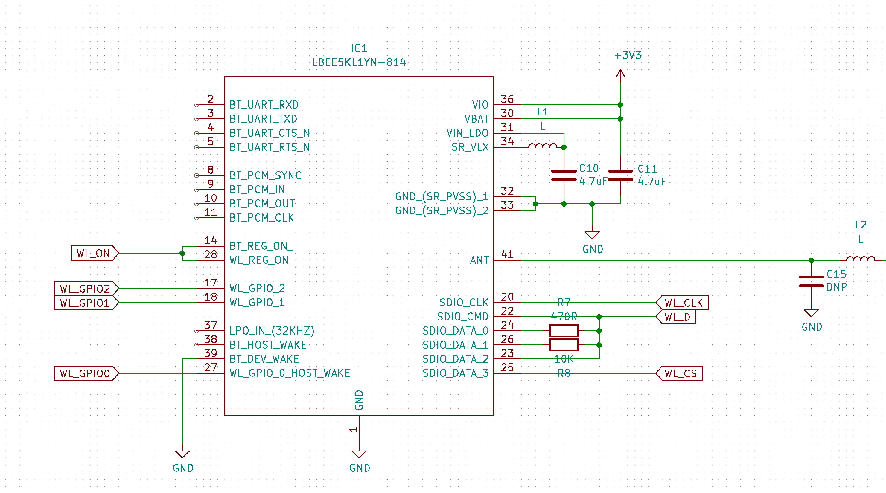
So RP2040 + WiFI, I wonder if there exists an easy-to-use and should-be high-bandwidth solution…. Oh yeah, the PicoW. The issue is that the PicoW form factor doesn’t fit well to my design (board size). I want to keep the enclosure as small as possible while it will be surrounded by aluminium and will be really bad with its antenna design. Now, if we look at the actual chipset PicoW is using, CYW43439, you can actually find a few modules that are using the same one. One of the modules, and probably the smallest one, is Murata’s Type 1YN. I have had the idea of using it to build PicoW for sometime now, and I actually have a few modules lying around already, so now is a perfect time to use it in a project.
If you look at the PicoW, you can see how they are connecting. It is actually quite interesting because the RP2040 does not have enough GPIO for a typical SDIO interface with signals like interrupts if you want to keep the same Pico form factor and pins available. There are only three GPIO + one power control used: WL_CLK, WL_D, that merges all the SDIO’s CMD and Data lines and a WL_CS pin.
The next one is the GPS module, because I want to keep the enclosure waterproof. Originally, I had to put the GPS antenna on board along with the WiFi antenna. I ignore the WiFi for now. Even if I have the GPS antenna by itself, it will not be in an optimal position in this CNC enclosure. So, an additional GNSS frontend is called in for SAW filter and LNA support. To my surprised, this GPS actually works in the enclosure along with WiFi.
Because this board will be the Geophone replacement sensor, I’m going to use the doorbell 24V AC to power it so I can put it outside and underground while still powering it without drilling another hole in the wall, so that is why there is a weird-looking capacitor bank and a full bridge on board. Though in a later revision, I decided to remove that (More on the reason for revision later).
Lastly but not the least, see if you can see what’s going on here:
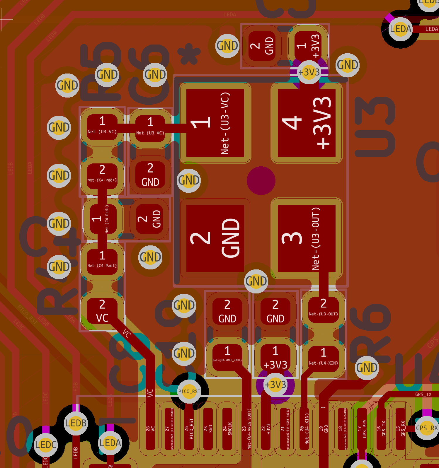
Usually, you’ll have a 12MHz oscillator for the RP2040, but since I need to align the timing with UTC and provide a stable 32KHz clock for the IMU, I found a VCTCXO that I can adjust the frequency of while still being a temperature-compensated oscillator for a stable clock. This 12MHz clock is used for the RP2040, and there’s a PWM DAC that can control small frequency changes to ensure the clock follows GPS (i.e., GPSDO).
For the case design, there are three M8 screw for the vibration damping mounts commonly used in audio speaker.
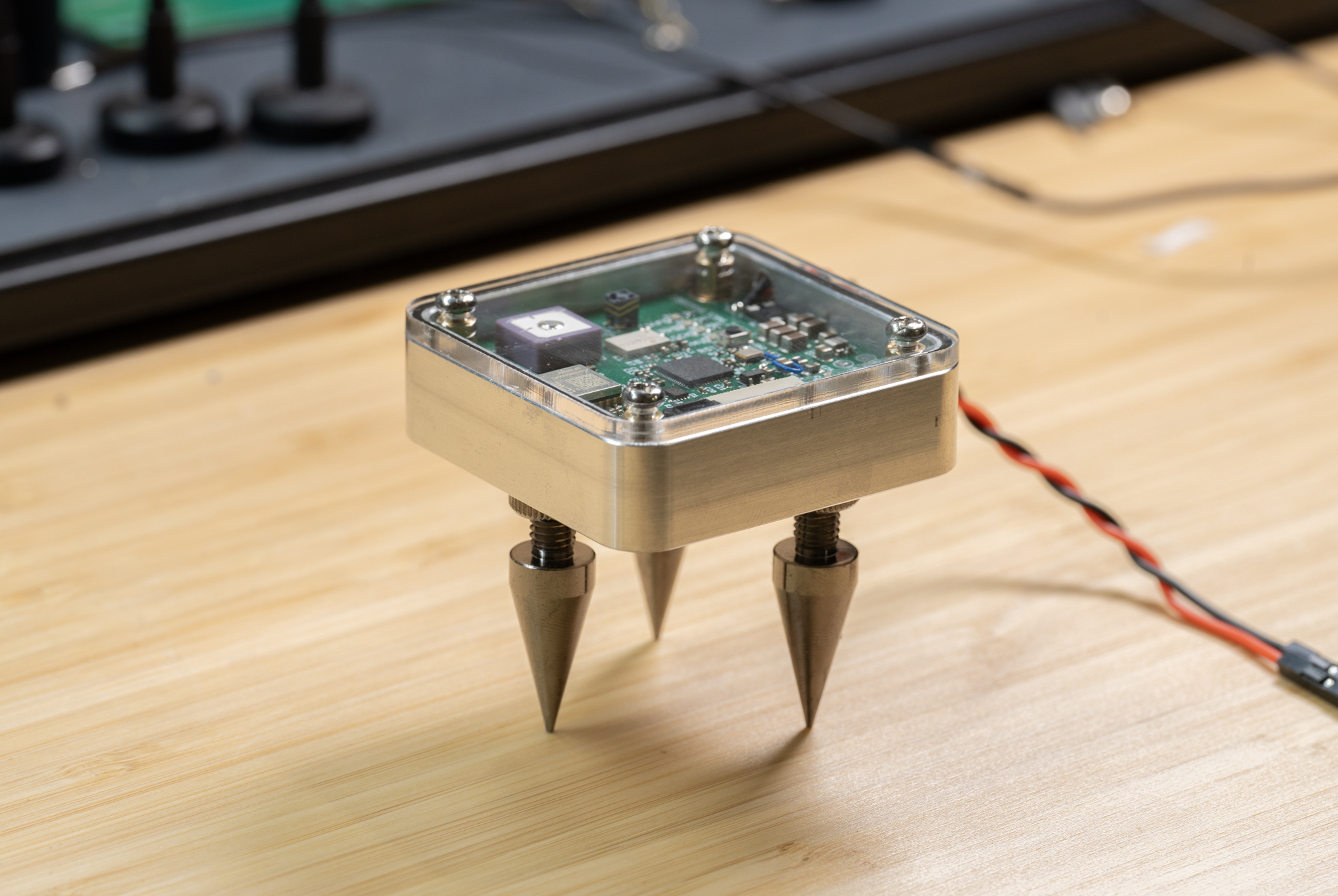
Once again, I would like to thank PCBWay for sponsoring this project. You can now order both the PCB and the CNC case directly from here.
Sidenote: It might be hard to find the 12Mhz VCTCXO, so you can go with TCXO like ECS-TXO-2520MV as a substitute.
MicroPython, CircuitPython, C SDK
Originally, when bringing up the FPGA on the sensor board, I opted with CircuitPython, and I still think it is a great decision because it emulates a USB drive and automatically reloads the program if the content has changed, which basically means my FPGA bitstream can be uploaded automatically if I copied the binary. Moreover, I can keep the exact binary format and have the CircuitPython code to read the file without converting it into things like C header files. Overall, I really like the setup when going through the brinup process.
One of the early issues though after I got the FPGA code done is how to send the data back for analysis. Originally, I thought it might be the performance bottleneck by CircuitPython printing the data to the USB serial interface. However, CircuitPython does not support the @native flag for optimizing the functions in native code. Additionally, one critical technical difficulty is that CircuitPython decides not to implement true interrupt support, so that means I can’t attach an interrupt routine for reading the IMU data using the IMU DRDY signal. Thus, I end up porting the code again to MicroPython.
So, this is during the bringup process and after I got the processing board back and started to bring it up, something weird happened: WiFi only works using CircuitPython and not in microPython, and what’s even more funny is that if I flashed CircuitPython and then microPython without power cycling the board, the first iteration in microPython will successfully initialize the WiFi.
So, here’s the thing: the MAC address isn’t programmed in the module, and by default in CircuitPython, if you don’t have it in the OTP, it’ll use a random MAC address. But it doesn’t work the same way in microPython for some reason. And I can’t seem to find a way to change program OTP memory either.
One thing I don’t like about microPython and CircuitPython is that they seem easy to use at first glance, but once you need to make changes to the underlying code (like enabling random MAC addresses in microPython), it can be a bit tricky to find the right place.
So, since the FPGA code is now stable, I’m going back to the C SDK and focusing on optimizing the performance. But I do want to note that with overclocking (250Mhz), I can get micropython to send the full array data (32 IMUs) back to the host either through UDP at 100Hz or USB CDC. And I didn’t have to optimize the Python code much, which is pretty impressive.
Now, let’s talk about the WiFi bandwidth. UDP has shown its potential, sending the full data (32 IMUs) at 100Hz. But I’m going with TCP here because I don’t want to miss any data. And it’s surprising how much it slows down with TCP.
LWIP has a tcp_write function, but it doesn’t send the package immediately. The tcp_output function is the flush command. If I flush out the data every time there’s a 512-byte packet, the overall throughput will take a hit. And in a busy WiFi network, it might not send the packet for a second. Plus, increasing the buffer size to the maximum limits makes the code unstable. So, I’ve set up a FIFO in my code instead of relying on LWIP’s buffer.
After all this effort, I still end up with the same 100Hz full data sample rate through WiFi, and to be clear, it can handle about 250Hz of data, but there is not enough memory to buffer during the interruption of communication (It is WiFi after all, but it is worse then what I originally thought). This is the point where I think if I ever want to send out the entire raw IMU data, I might have to look elsewhere.
Analyzing the result
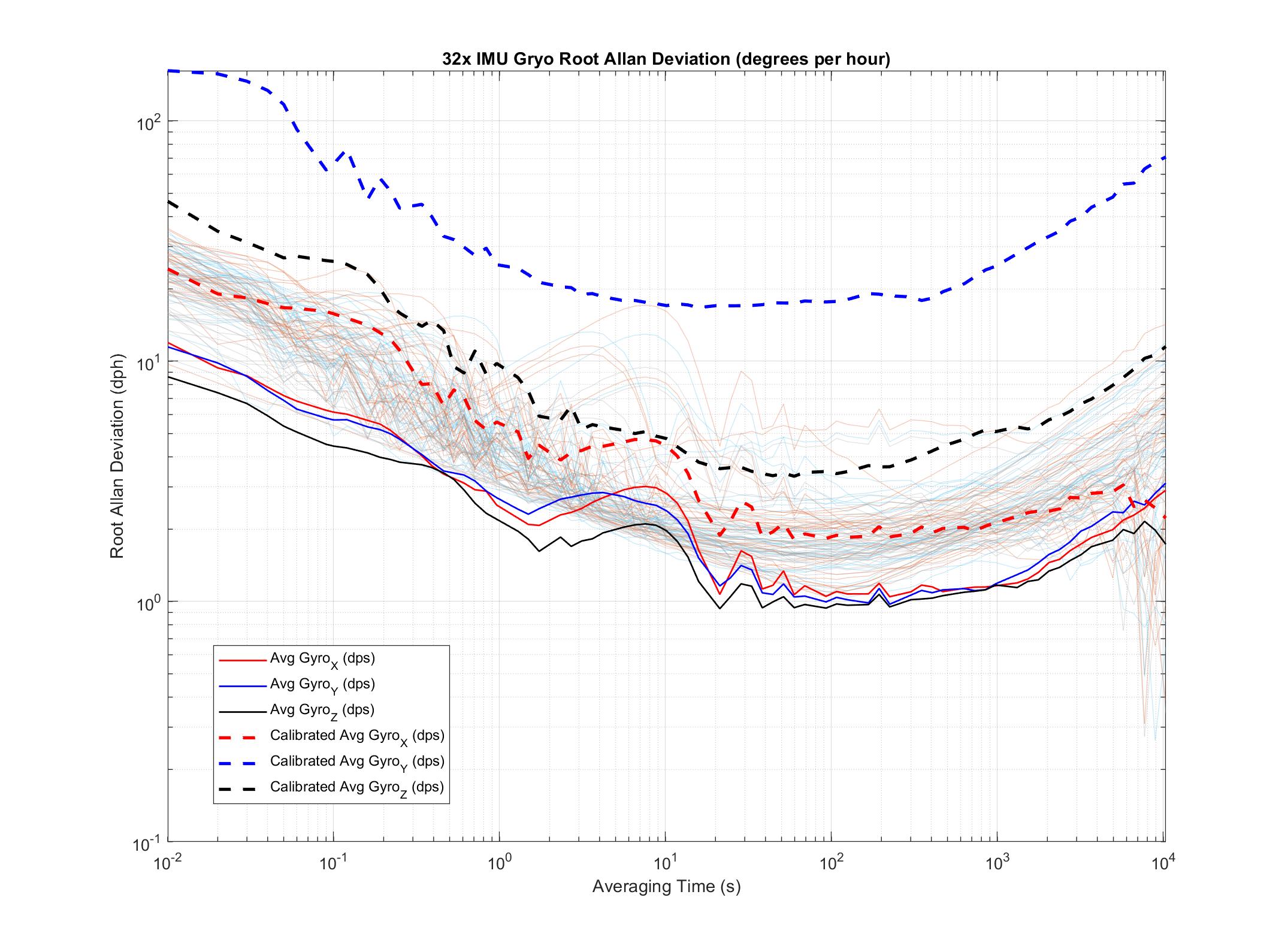
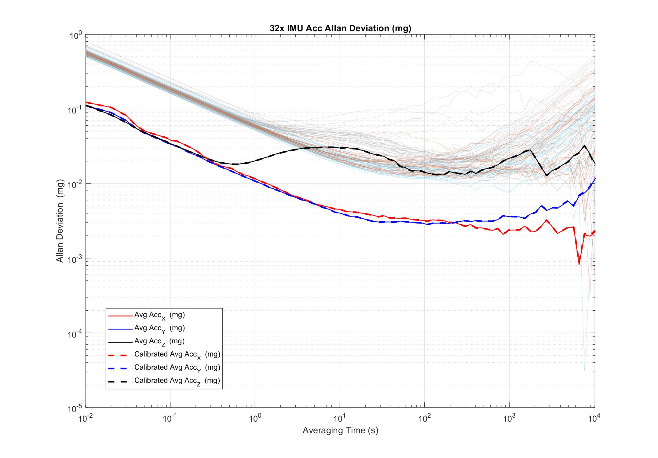
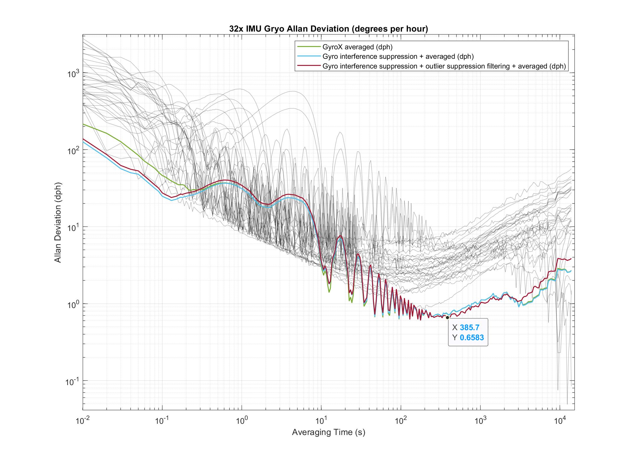
I’m still able to get long duration and full(all 32 IMU) data traces to analyze it’s performance in ADEV plot, and here I present some of the results. The test setup is putting the sensor on the floor while I’m away from my home to minitureized the vibration.
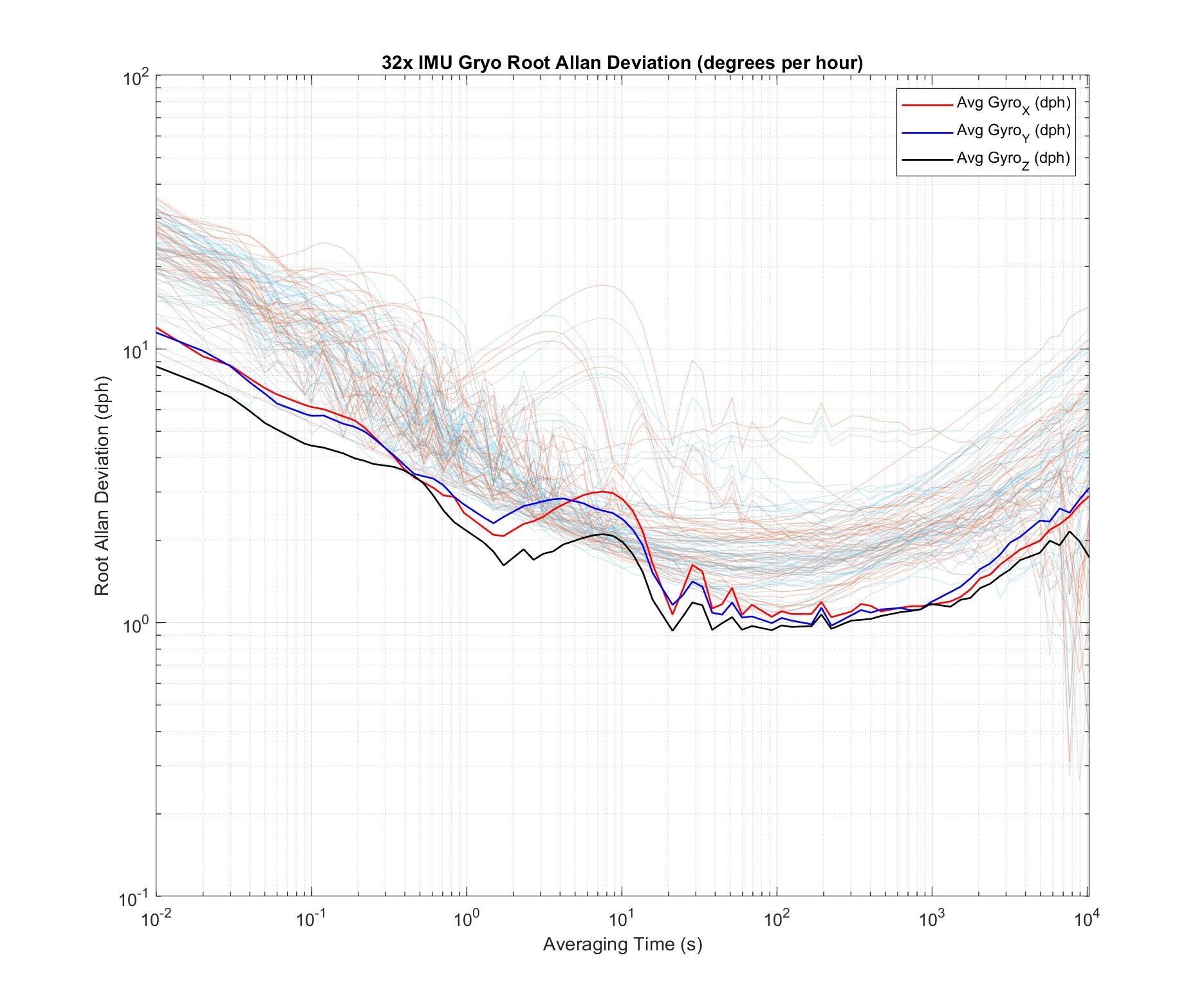
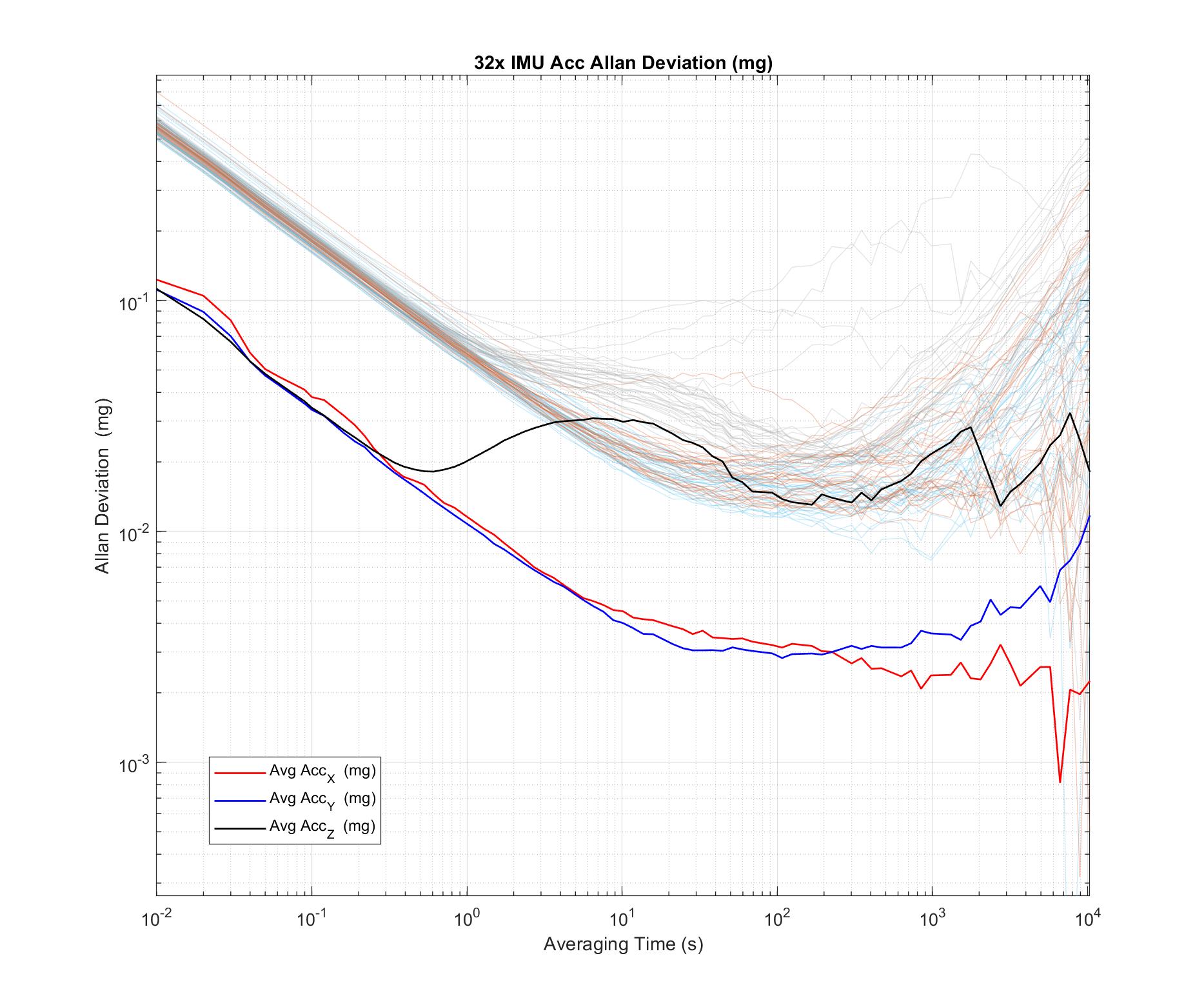
Let’s compare the result with Sony’s paper [2]:
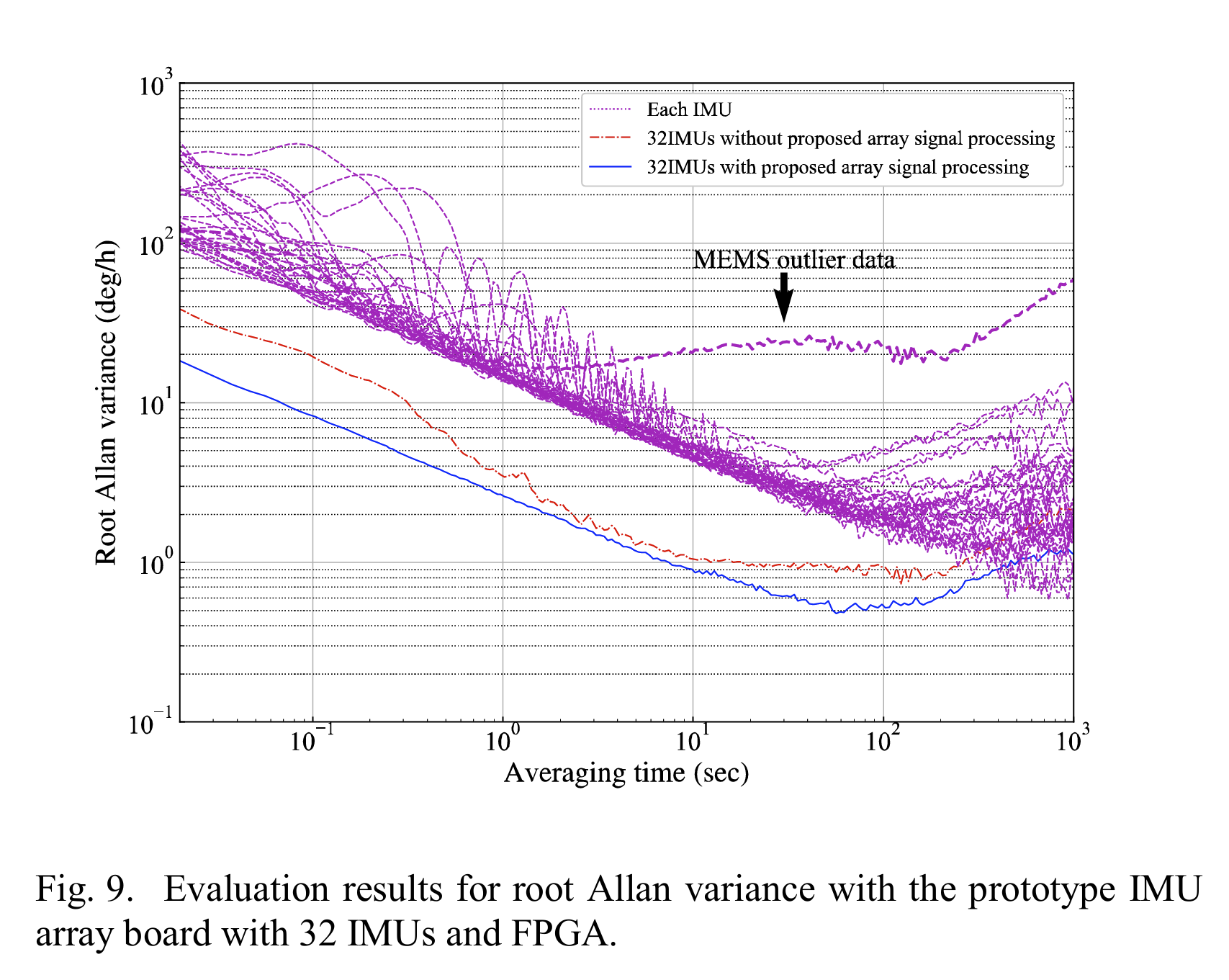
Kamata, Hiroyuki et al. “MEMS Gyro Array Employing Array Signal Processing for Interference and Outlier Suppression.” 2020 IEEE International Symposium on Inertial Sensors and Systems (INERTIAL) (2020): 1-4. Figure 9.
I do see some outlier data in my gyro plot (barely), while I can see there exists a different profile for Acc Z axis, which is somewhat expected because the Z axis design will be different on the MEMS chip comparing to other X/Y axis that is just rotated by 90 degrees. What’s even more interesting is that I did not see much gyro improvements from averaging multiple of them, though I do notice that stationary gyro data seems to be way noisy comparing to the dynamic data (slowly rotating the sensor).
What’s more is that I did try to implment the outlier suppression filtering and interference suppression filtering but both method doesn’t perform as well comparing to what the paper can achieve, specificlly in short duration the performance does able to improve but the difference disapared at 0.2s, at 300s the outlier supression even performed worse then just the averaging.
Even though replicating that part has failed (In my opinion), there is another one that thankfully is a success and it is important (to a lot of papers) - which is Calibration.
Calibration
Reference 5 is a interesting read, basically what they’ve shown is that even without a turntable, you can still calibrate the alignment for each IMU in the array, highly recommended to read through.
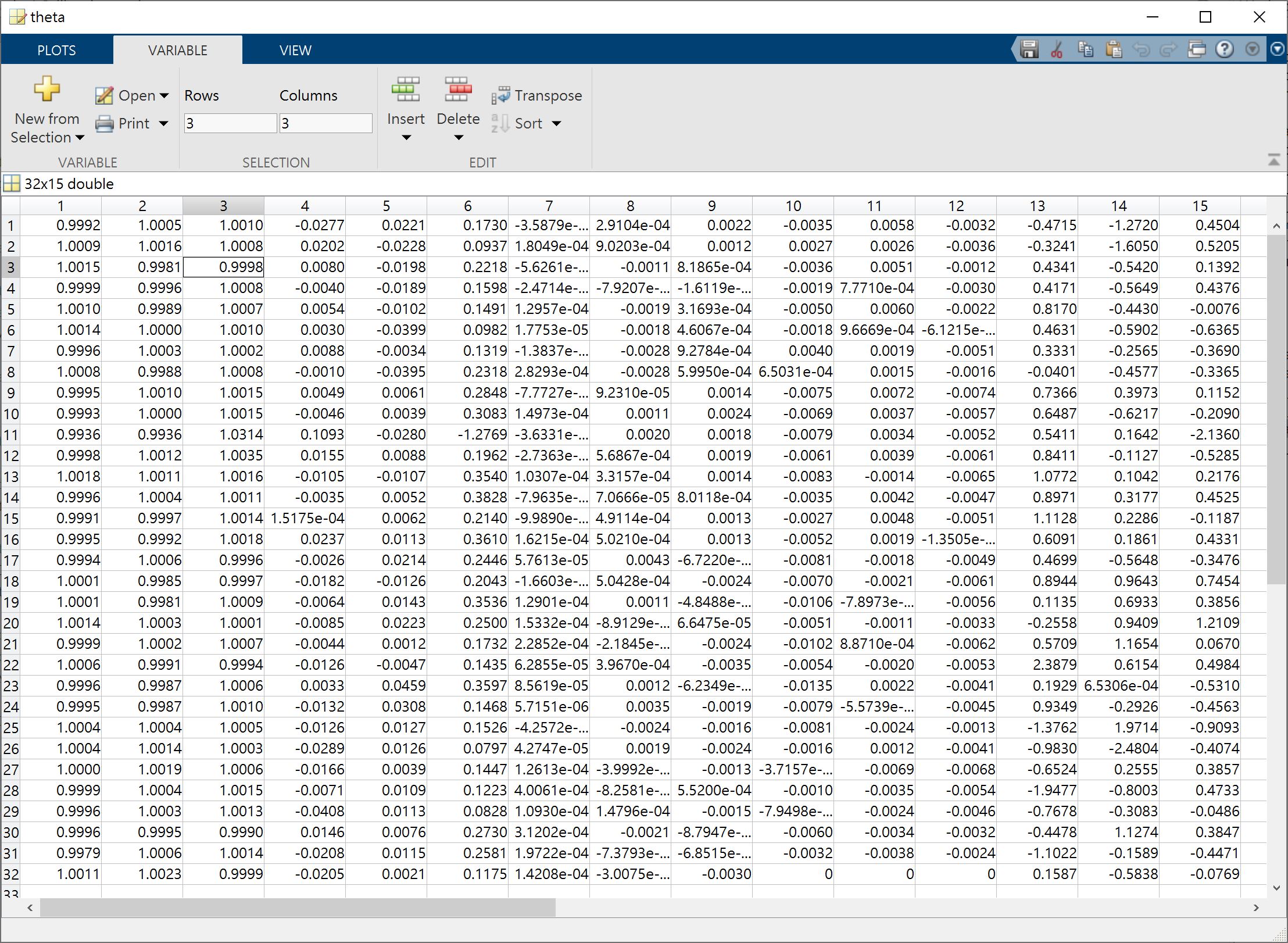
Following the paper, I’ve also 3D printed a Icosahedron with a slot to insert the sensor, and powered externally and then capture the data using UDP through WiFi. With 20 different position data and 90 seconds each, I’m able to calculate the misalignments and sensitiviety for each IMU.
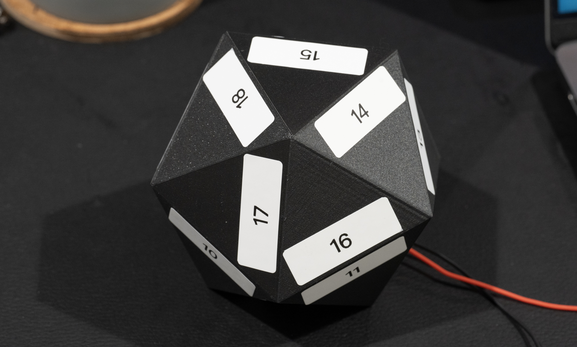
Following the paper’s matlab code, I also have a script to generate the header file for the sensor to calibrate the data in RP2040 and do sensor fusion (i.e averaging) and output the resulting calibrated data.
However, one of the issue I have is that… ADEV plot isn’t that better comparing to the uncalibrated result, this is probably because I’m not testing the sensor in a dynamic environments [Reference 4 section I-b].
Future Plan
Ethernet
First thing first - I want to have something else to transmit the data, with long range, time-sync (So I don’t need a GPS on-board) and easy to use.
That really goes down to ethernet with IEEE 1588 support, from my research a lot of the driver support is sketchy for MCUs, if I go with MAC + PHY, the best option will be W5500 but it doesn’t support IEEE 1588, LAN9250 is a similar option but it’s FULL driver isn’t available. Another similar-ish options will be using single-pair ethernet, LAN8651 has a better driver (It looks like), and ADIN1110 will be better (For me) since it is 10Base-T1L that means longer range. The only thing that I’m worried about is the bandwidth, even though the line rate is at 10Mbps, I’m not quite sure what is the actual achieveable datarate with like… 512bytes per package.
If I go with PHY only, the option I guess is to use ESP32 as host which it supports RMII PHYs, and searching do shows that there are some options for 100Base-T that will be easier to use then SPE which will requires a adaptor to connect it to any common wired ethernet systems. So rightnow I’m still thinking which route to go.
Sensor board
For the sensor board itself, as for now I don’t really have a plan to update, because like I wrote earlier that the point of the sensor board is to reuse it as much as possible so I don’t have to pay another costly PCBA. But if anyone is thinking about it, I’ll suggest using RP2350 + SPE. During the designing phase I keep thinking about using RP2040 directly communicate with the IMUs but it just doesn’t have enough GPIOs, also external flash puts another burdon in the layout, and after two weeks I got the board back/bring up, RP2350 announsed, yeap.
V1.1
Though given that now I do want a USB connector on the case for reliable connection, I have a quick update to the board and case design.
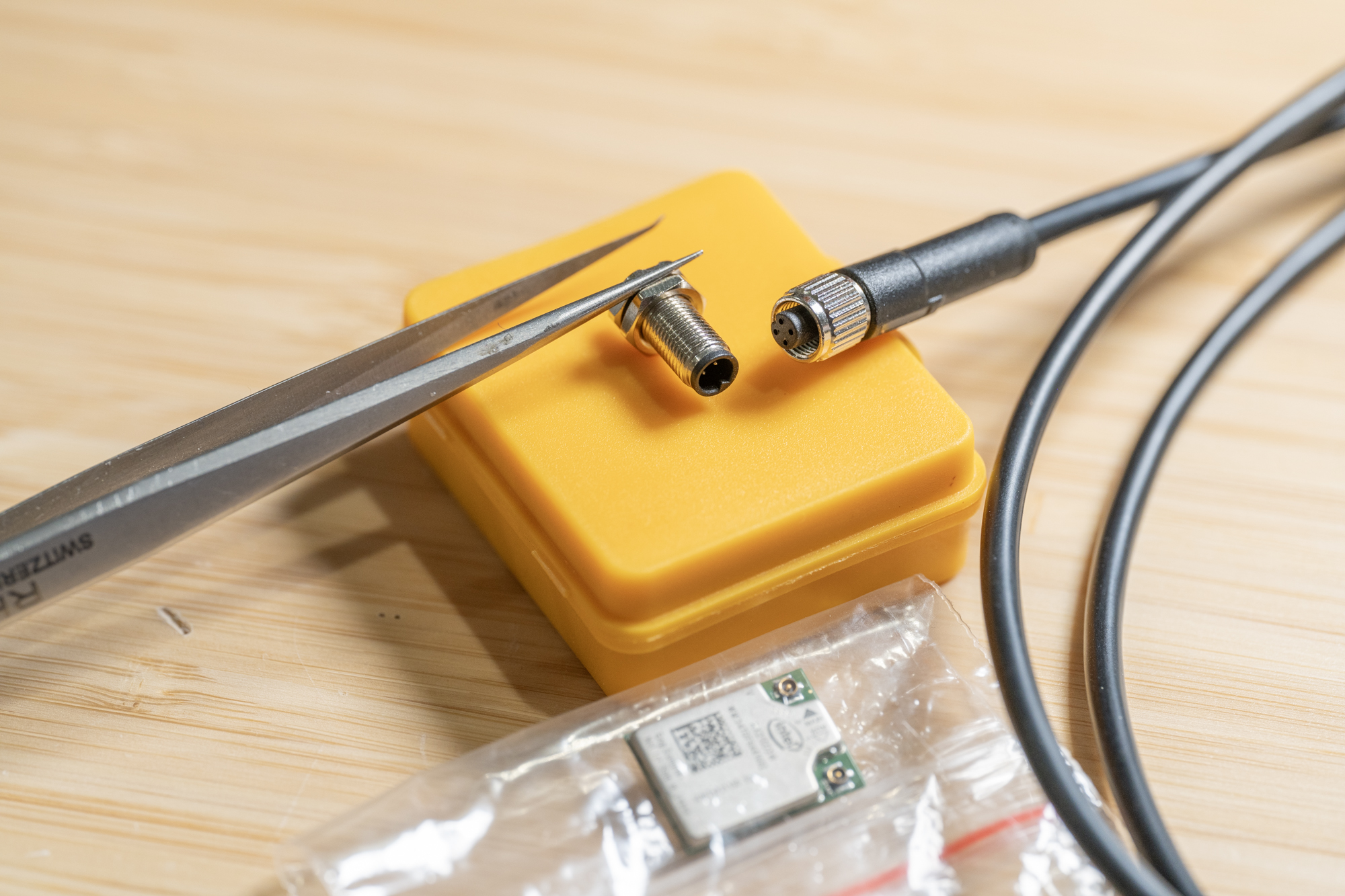
With a bunch of time searching for the perfect connector, I finally got this 4-pin M5 screw-in waterproof connector.
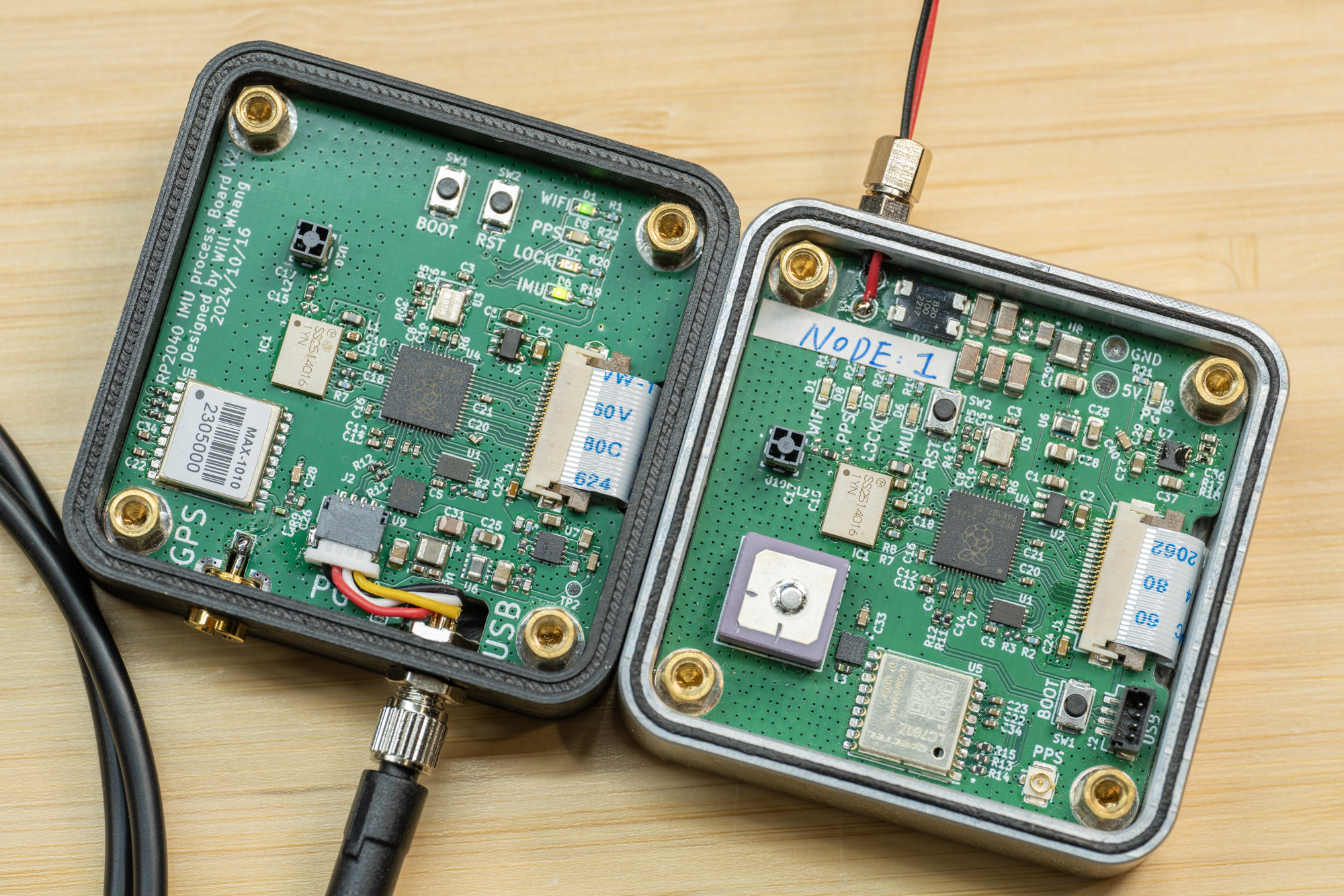
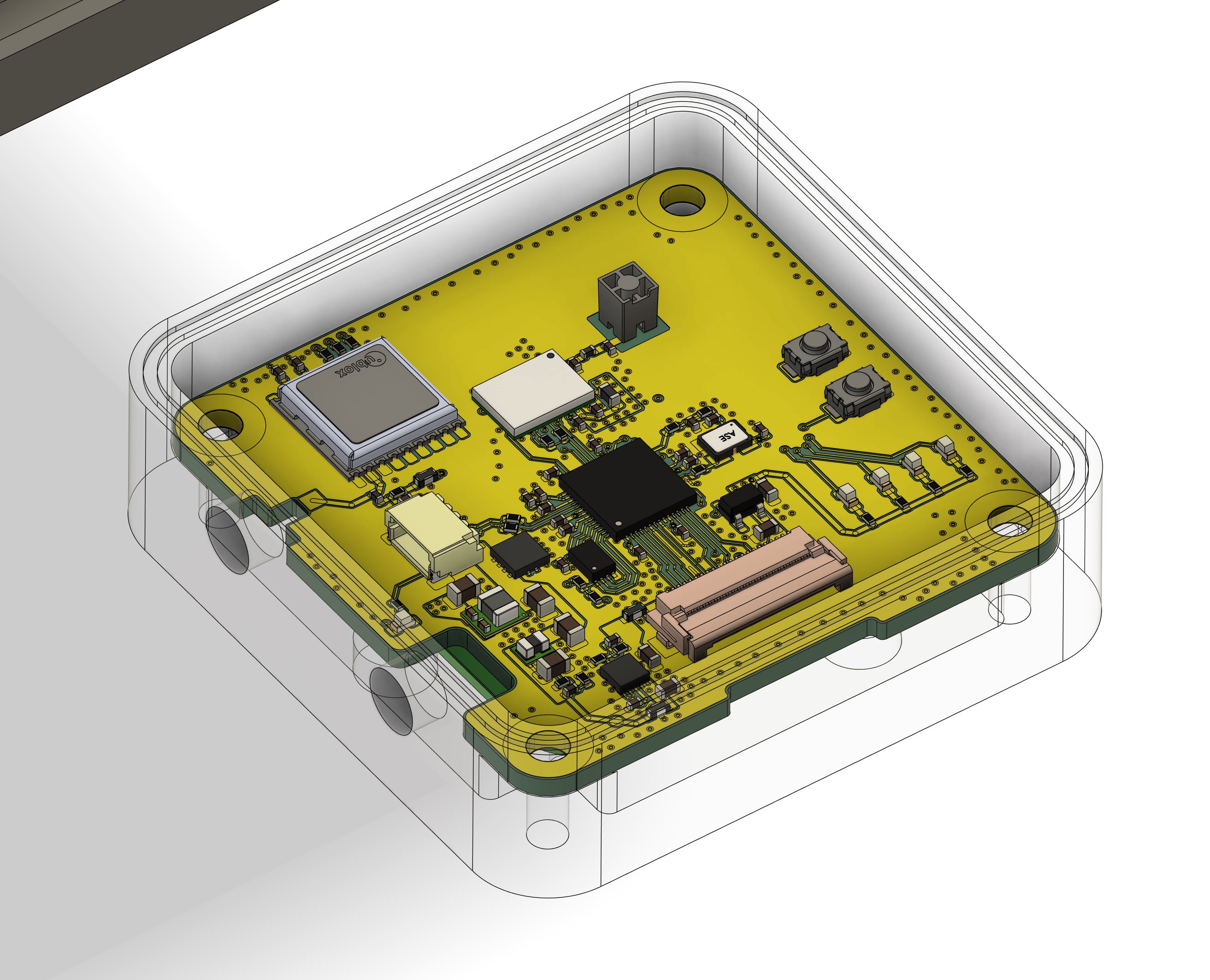
Here is the board V1.1 in the 3D printed case for fit testing before I send the file to PCBway, you can see that the connector barely fit but the GPS antenna connector is perfect. (yeah I remove the internal GPS antenna also because I might bury it under ground yet again).
Cross comparison with Geophone
Finally given the code is done, I’m going to deploy this sensor and do a comparison with the geophone data and see how it performs.
Sponsor

Again, thank you PCBWay for sponsoring this project!
Here are the links to PCBWay project site:
IMU_Array_Processing_board
IMU_Array_Sensor_board
Here is the Github repo for all the board design file/source code. Github
References & Inspiration
Here are some of the reference during this … ah… research, I’m not writing a paper here just FYI.
[1] Sony SPRESENSE IMU array board
[2] Kamata, Hiroyuki et al. “MEMS Gyro Array Employing Array Signal Processing for Interference and Outlier Suppression.” 2020 IEEE International Symposium on Inertial Sensors and Systems (INERTIAL) (2020): 1-4. Link
[3] Blocher, Lukas et al. “Purely Inertial Navigation with a Low-Cost MEMS Sensor Array.” 2021 IEEE International Symposium on Inertial Sensors and Systems (INERTIAL) (2021): 1-4. Link
[4] Wang, Liqiang et al. “Improving the Navigation Performance of the MEMS IMU Array by Precise Calibration.” IEEE Sensors Journal 21 (2021): 26050-26058. Link
[5] Nilsson, John-Olof et al. “Aligning the Forces—Eliminating the Misalignments in IMU Arrays.” IEEE Transactions on Instrumentation and Measurement 63 (2014): 2498-2500. Link
Leave a comment